

Trade-off Analysis Between Insertion Loss and Bandwidth in High-Power Cavity Bandpass Filters
Abstract
The high-power cavity bandpass filter is an indispensable frequency-selective component in the transmit chains of 5G base stations, wireless repeaters, and satellite ground stations. It must handle kilowatt-class peak power while keeping the in-band insertion loss (IL) as low as possible. However, an unavoidable physical boundary exists between insertion loss and bandwidth: at a fixed cavity unloaded Q (Qu), the narrower the bandwidth and the higher the selectivity, the greater the insertion loss. In high-power scenarios, every decibel of insertion loss converts directly into heat dissipation inside the cavity, threatening frequency stability and long-term reliability. Starting from the S21 parameter, this paper establishes a quantitative IL–Qu–FBW trade-off model, dissects the contributions of conductor loss, dielectric loss, and plating technology, addresses thermal management, PIM, and electrical breakdown issues unique to high-power design, and concludes with Temwell specifications and a design strategy matrix that provides actionable engineering optimization paths.
1. Introduction: The Strict Low-Insertion-Loss Demand of High-Power Applications
1.1 High-Power Application Scenarios: Base Stations and Repeaters
In 5G New Radio (NR) mobile networks, the macro-cell base station is the workhorse of coverage. The average output power of the transmit power amplifier (PA) of a single sector typically falls in the 40–80 W range; under a peak-to-average power ratio (PAPR) of 8–10 dB, the instantaneous peak power can reach hundreds of watts. The cavity bandpass filter positioned after the PA and before the antenna must carry the transmit signal at this power level while simultaneously suppressing adjacent-channel spurious signals and receive-band interference. Wireless repeaters, distributed antenna systems (DAS), satellite ground stations, and public-safety radio (TETRA/P25) transmit front-ends face similar conditions.
In these scenarios, low insertion loss is not a nice-to-have but a hard line in the system specification, for three reasons: First, transmit efficiency — every additional 1 dB of filter IL means roughly 21% of PA output power is wasted. Second, system coverage and receive sensitivity — the front-end filter's IL degrades the system noise figure (NF) in an almost 1:1 ratio. Third, thermal reliability — the consumed power becomes heat inside the cavity, which is the most fundamental difference between high-power design and ordinary signal-level filter design.
1.2 The Core Conflict and Research Objective
The core conflict of filter design is that the engineer is simultaneously required to deliver "narrow bandwidth, high selectivity" and "low insertion loss," and these two are physically opposed. Narrow bandwidth means energy must dwell longer inside the cavity and reflect back and forth more times; each reflection deposits some loss in the metal walls and dielectrics, causing passband insertion loss to rise steeply as bandwidth narrows. The only escape is to raise the cavity's energy-storage efficiency — i.e., increase the unloaded Q — but high Q typically means larger volume, more expensive plating processes, and tighter mechanical tolerances.
For high-power systems, this conflict is further amplified. Insertion loss has a dual identity: it is both the attenuation of the signal and the heat source of the cavity. The objective of this paper is to build an analytical framework spanning physical mechanisms, quantitative models, and engineering practice, providing actionable optimization strategies for RF engineers.
2. Definition of Insertion Loss: Interpreting the S21 Parameter
2.1 The S21 Parameter and the Definition of Insertion Loss
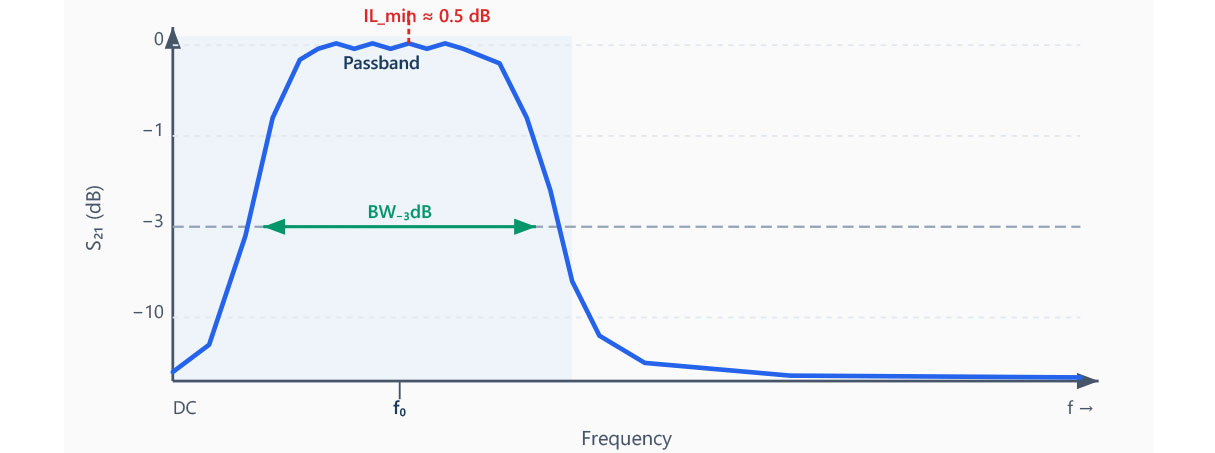
Insertion loss is the most direct metric of the passband efficiency of a filter, defined as the power lost by the signal after passing through the filter, expressed in decibels. Within the S-parameter framework of a two-port network, insertion loss is the logarithmic measure of the S21 magnitude:
An ideal lossless filter has |S21| = 1 in the passband, corresponding to IL = 0 dB; in reality, metallic conductor resistance, dielectric loss tangent, and connector contact resistance all make |S21| less than 1. Figure 1 uses a 4-pole Chebyshev response to illustrate the relationship among IL_min, the −3 dB reference, and the passband interval.
2.2 The Ideal Value of ≤ 0.5 dB versus the Practical Range
"The lower the insertion loss, the better" gives the direction, but engineering needs an operable yardstick. For cavity bandpass filters, the industry generally grades passband insertion loss as follows:
| Rating | IL Range | Typical Application | Engineering Implication |
|---|---|---|---|
| Excellent | ≤ 0.5 dB | Satellite Tx front end, high-power macro cell | Near the material physical limit; needs high-Qu cavity |
| Good | 0.5 – 1.0 dB | 5G macro cell, wireless repeater | Practical target range for high-power design |
| Acceptable | 1.0 – 2.5 dB | Wideband receive, mid/low-power systems | Heat dissipation and NF impact must be assessed |
| Caution | > 3.0 dB | Not advised for high-power or high-sensitivity | Loss and heating too large; usually a poor design |
The ideal value of ≤ 0.5 dB is mostly seen in satellite and military-grade applications where bandwidth is ample and cavity Qu is extremely high. For 5G Sub-6 GHz macro cells constrained by spectrum congestion and volume, "typical ≤ 0.7 dB, maximum ≤ 1.0 dB" is a reasonable engineering baseline for the high-power version. Once the spec falls above 1.5 dB, heat-sinking design must be reviewed simultaneously.
2.3 Clarifying Insertion Loss versus Stopband Rejection
Insertion loss is measured inside the passband — its ideal direction is toward 0 dB, describing how much of the useful signal is consumed. Stopband rejection is measured outside the passband — its ideal direction is as large as possible (e.g., > 60 dB), describing how much of the interfering signal is suppressed. A filter that achieves steeper, deeper stopband rejection typically requires stronger coupling or more poles, both of which push up passband insertion loss. In other words, "blocking the unwanted more cleanly" and "passing the desired more smoothly" are two sides of the same coin — this is the recurring trade-off axis throughout the rest of this paper.
3. Factors Affecting Insertion Loss: Conductor Loss, Dielectric Loss, and Cavity Q
3.1 The Two Loss Mechanisms: Conductor Loss and Dielectric Loss
The passband insertion loss of a cavity filter physically arises from two dissipation paths. The first is conductor loss: RF current flows on the metallic inner wall and, constrained by the skin effect, concentrates within a skin depth only a few micrometers thick, giving an equivalent resistance far greater than the DC resistance. The higher the frequency, the more severe the conductor loss; inner-wall surface roughness, oxidation, and plating material all significantly alter this dissipation. The second is dielectric loss: if dielectric resonators or support pieces are present, the loss tangent (tan δ) continuously converts energy stored in the electric field into heat. For air-filled cavities, dielectric loss is negligible and conductor loss dominates.
Two minor paths often overlooked are radiation loss (energy leaking through seams or openings) and contact loss at connectors and joints. In high-power scenarios, the latter is especially critical — minor oxidation or poor contact not only increases insertion loss but is also a breeding ground for passive intermodulation (PIM).
3.2 The Unloaded Q (Qu)
All the loss paths above can ultimately be condensed into a single quality metric — the unloaded Q of the resonant cavity, defined as the ratio of energy stored to energy dissipated per oscillation cycle:
The higher the Qu, the better the cavity "holds energy and leaks little," with correspondingly lower insertion loss and stronger frequency selectivity. The inherent Qu gap between different filter technologies is enormous:
| Filter Technology | Typical Qu | Typical IL | Freq. Range | High-Power Suitability |
|---|---|---|---|---|
| Lumped LC | 50 – 200 | 1 – 6 dB | DC – 3 GHz | Low (high loss, high heating) |
| Microstrip filter | 100 – 300 | 2 – 5 dB | 0.5 – 30 GHz | Low |
| SAW / BAW | 500 – 2,000 | 1 – 4 dB | 0.1 – 6 GHz | Low (limited power handling) |
| Cavity filter | 1,000 – 20,000 | 0.2 – 2 dB | 0.1 – 60 GHz | High (mainstream choice) |
| Dielectric resonator | 5,000 – 50,000 | 0.2 – 1 dB | 0.5 – 40 GHz | Med-high (narrowband, high Q) |
3.3 The Core Formula: The Triangular Relationship of IL, Qu, and Bandwidth
For a multi-pole bandpass filter with center frequency f₀ and 3 dB bandwidth BW, the minimum insertion loss at the passband center is approximately:
where Σgᵢ is the sum of the low-pass prototype element values (~4.3 for a 4-pole 0.1 dB-ripple Chebyshev), Qu is the unloaded Q, and FBW = BW/f₀ is the fractional bandwidth. This formula condenses the entire thrust of this paper:
- FBW decreases (bandwidth narrows) → denominator shrinks → IL rises; this is the mathematical root of "narrow bandwidth pays a loss penalty."
- Qu increases (cavity quality improves) → denominator grows → IL falls; this is the value of high-Q design.
- Σgᵢ increases (more poles) → numerator grows → IL rises; this is the "selectivity-for-loss" penalty (see Section 4).
3.4 The Influence of Conductor Material and Surface Plating
Since conductor loss largely dominates the Qu of an air cavity and the skin effect confines current to an extremely thin surface layer, the "surface material" influence far exceeds that of the cavity body material. Silver plating on the inner wall can raise Qu by 15–30% relative to bare copper without changing cavity dimensions. Figure 2 compares different surface treatments' Qu and their corresponding insertion loss (at FBW = 0.5%, 4-pole conditions).
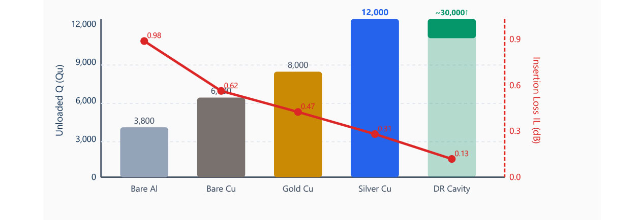
From bare aluminium to silver-plated copper, Qu rises from ~3,800 to ~12,000, and at FBW = 0.5% the insertion loss drops from ~0.98 dB to ~0.31 dB — roughly a threefold improvement. For high-power design, silver plating also provides good oxidation-resistance contact characteristics, helping reduce PIM. Gold plating may be considered for humid or salt-spray environments. Material selection is always a holistic trade-off among conductivity, oxidation resistance, PIM performance, and cost.
4. The Cost of Bandwidth Extension: Pole Count and the Physical Mechanism of Rising Insertion Loss
4.1 The Bandwidth–Insertion-Loss Trade-off Curve
Plotting the core formula against FBW yields the one decision chart engineers need most. Figure 3 plots "minimum insertion loss vs. fractional bandwidth" for four values of Qu in a 4-pole Chebyshev design.
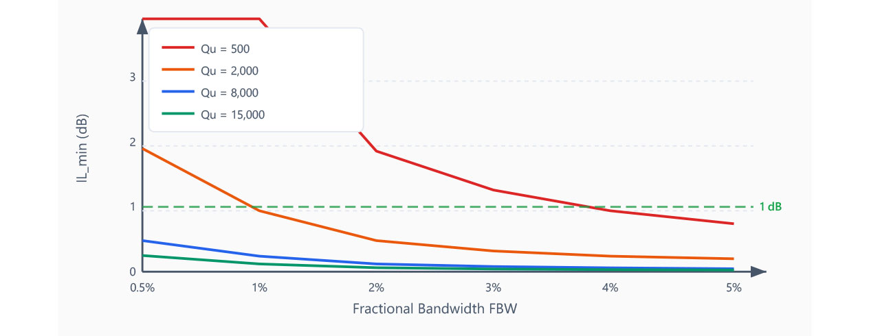
Three observations deserve every RF engineer's attention. First, every curve rises steeply as bandwidth narrows — when FBW shrinks from 5% to 1%, the IL is amplified exactly fivefold at the same Qu. Second, the vertical spacing of the curve family quantifies the value of Qu: at FBW = 2%, Qu = 500 gives IL = 1.87 dB whereas Qu = 8,000 gives only 0.12 dB. Third, the green high-power IL limit line divides the design space — only designs below the line are viable.
| Fractional BW | Qu = 500 | Qu = 2,000 | Qu = 8,000 | Qu = 15,000 |
|---|---|---|---|---|
| 5% | 0.75 dB | 0.19 dB | 0.047 dB | 0.025 dB |
| 2% | 1.87 dB | 0.47 dB | 0.12 dB | 0.062 dB |
| 1% | 3.74 dB | 0.93 dB | 0.23 dB | 0.12 dB |
| 0.5% | 7.47 dB | 1.87 dB | 0.47 dB | 0.25 dB |
4.2 The Physical Mechanism and Loss Penalty of Adding Poles
Beyond the bandwidth–IL trade-off lies a second axis: selectivity vs. insertion loss. Each added pole increases stopband roll-off by ~20 dB/decade, but the signal must traverse one more lossy resonant cavity, accumulating more passband IL.
| Pole Count N | Stopband Roll-off | IL Increment | Volume / Cost | Typical Application |
|---|---|---|---|---|
| 2 poles | ~40 dB/dec | Baseline | Small | General selectivity, spurious suppression |
| 4 poles | ~80 dB/dec | +50 – 100% | Medium | Mainstream 5G base-station front end |
| 6 poles | ~120 dB/dec | +100 – 150% | Large | High-selectivity macro cell, repeater |
| 8 poles | ~160 dB/dec | +150 – 200% | Largest | Satellite, radar, and other demanding uses |
Key design tip: for the same selectivity requirement, "moderate pole count + transmission zeros" often has lower IL than "high pole count without zeros." Transmission zeros (TZs), created through cross-coupling between non-adjacent resonant cavities, create deep rejection notches at specific stopband frequencies — one of the few tools that can bypass the selectivity–IL trade-off.
4.3 Coupling Strength: The Tuning Knob for Bandwidth
Besides pole count, coupling strength is another design variable that directly affects bandwidth and insertion loss. The size of the coupling iris or coupling loop determines the energy exchange rate between adjacent resonant cavities: stronger coupling widens the 3 dB bandwidth and slightly lowers passband IL, but flattens the skirt and reduces selectivity; weaker coupling narrows bandwidth, raises IL, and steepens the skirt. For engineers, coupling amount, pole count, and Qu are three knobs that must be adjusted together — adjusting any one alone shifts the balance between bandwidth and insertion loss.
5. Special Considerations for High-Power Design: The Effect of Thermal Management on Insertion-Loss Stability
5.1 Insertion Loss Is Heat Dissipation
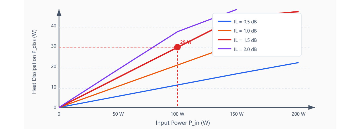
In a high-power transmit chain, insertion loss acquires physical weight — heat. The power consumed by the filter turns into heat-dissipation power inside the cavity, calculated exactly as:
This is the one formula in high-power design that most deserves to be memorized yet is most often underestimated. Figure 5 plots heat-dissipation power against input power for different insertion losses, marking a typical scenario: at 100 W input and IL = 1.5 dB, about 29 W is dissipated as heat inside the cavity.
| Input Power | IL = 0.5 dB | IL = 1.0 dB | IL = 1.5 dB | IL = 2.0 dB |
|---|---|---|---|---|
| 20 W | 2.2 W | 4.1 W | 5.8 W | 7.4 W |
| 50 W | 5.4 W | 10.3 W | 14.6 W | 18.5 W |
| 100 W | 10.9 W | 20.6 W | 29.2 W | 36.9 W |
| 200 W | 21.7 W | 41.1 W | 58.4 W | 73.8 W |
5.2 The Effect of Thermal Effects on Insertion-Loss Stability and Frequency Drift
The harm of heat dissipation lies not only in temperature itself but in the fact that it turns back to degrade the filter's electrical performance, forming a negative feedback chain. First, conductor resistance increases with rising temperature: metal resistivity has a positive temperature coefficient (~+0.4%/°C for copper), causing Qu to fall, insertion loss to rise further — if heat-sinking is inadequate, thermal runaway may result. Second, cavity thermal expansion shifts the resonant frequency, potentially causing passband-edge signals to fall on the skirt and suffer additional attenuation.
Therefore, the specification of a high-power cavity bandpass filter must cover the entire operating temperature range. Temwell's engineering guideline: at maximum operating temperature, thermal IL drift ΔIL < 0.3 dB and center-frequency drift Δf < ±0.1%·f₀. Means of achieving this include low-CTE cavity materials, temperature-compensation structures, and high-temperature burn-in testing before shipment.
5.3 Passive Intermodulation and Electrical Breakdown
High-power scenarios involve two reliability issues indirectly related to insertion loss. The first is Passive Intermodulation (PIM): when a high-power signal flows through metallic junctions with poor contact, oxidation, or nonlinearity, intermodulation products are generated; if these fall into the receive band, they directly raise the noise floor. Silver-plated inner walls with precision mechanical contact are key to suppressing PIM; any measure that sacrifices joint quality to lower insertion loss tends to be punished by PIM degradation. The second is electrical breakdown: electric-field concentration points inside the cavity (e.g., tuning screw tips) may ionize air under high peak power, especially at high altitude (low pressure). Cavity dimensions must match the power density and sharp corners should be rounded.
6. Temwell Specifications: Typical IL Specs and Measurement Methods
6.1 Insertion-Loss Measurement Method
Insertion loss is measured with a vector network analyzer (VNA) as the standard instrument. Before measurement, the VNA must first be two-port calibrated with SOLT (or equivalent) standards to remove the influence of test cables, connectors, and fixtures, so that the reference plane falls accurately at both filter ports — a critical step, since fixture loss would otherwise be incorrectly attributed to the filter. After calibration, scan the frequency range covering the passband; read the minimum S21 in the passband as IL_max, and the passband average as IL_typ.
For high-power products, in addition to small-signal S21 measurement, Temwell also performs loaded testing at rated power, measuring the IL thermal drift ΔIL at thermal equilibrium and the PIM product level under dual-carrier excitation, ensuring the product meets specifications at actual transmit power and operating temperature.
6.2 Typical Specifications of Temwell High-Power Cavity Bandpass Filters
| Specification Item | Typical Range / Value | Design Note |
|---|---|---|
| Frequency range | DC to 60 GHz (model-dependent) | Covers 5G Sub-6 GHz bands and FR2 mmWave |
| Bandwidth config | 1 MHz to 40 GHz selectable | From narrowband high-selectivity to wideband, all customizable |
| Insertion loss (typ.) | ≤ 0.7 dB (high-power version) | Silver-plated cavity + high-Qu design |
| Insertion loss (max.) | ≤ 1.0 dB | Guaranteed value over full temperature range |
| Stopband rejection | Up to ≥ 60 – 80 dB | Depends on pole count and TZ configuration |
| Power handling | 100 W class and above | Supports macro-cell transmit-chain CW power |
| PIM performance | Low PIM (silver plating + precision contact) | Meets base-station receive-band noise-floor requirements |
| Connector type | SMA / N-type / custom | Selected per system interface requirements |
| Temperature stability | ΔIL < 0.3 dB, Δf < ±0.1%·f₀ | Verified by high-temperature burn-in |
6.3 Design Strategy Matrix
| Design Goal | Recommended Strategy | Expected Result |
|---|---|---|
| Lowest insertion loss | Raise Qu (silver plating, larger cavity); relax bandwidth; reduce pole count | IL approaching 0.3 – 0.5 dB |
| Highest selectivity | Add poles or TZs; accept slightly higher IL; reinforce heat sinking | Stopband ≥ 70 dB, IL 1.0 – 2.0 dB |
| High-power stability | Hold IL ≤ 1 dB; complete heat-sinking and TIM; low-PIM plating | ΔIL < 0.3 dB, long-term reliable |
| Bandwidth and low IL together | Choose Qu > 5,000 cavity; use TZs to trade for fewer poles | FBW 2 – 5%, IL ≤ 0.7 dB |
| Narrowband high selectivity | Use dielectric resonator; strict mechanical tolerance and temp. compensation | FBW < 1%, IL ≤ 1 dB |
7. Conclusions: Engineering Strategies for Insertion-Loss Optimization
The design of a high-power cavity bandpass filter is, in essence, the search for the optimal point within the trinary trade-off formed by insertion loss, bandwidth, and selectivity; there is no free lunch. The analysis of this paper condenses into the following five engineering conclusions.
Understanding this triangular relationship of Qu, bandwidth, and insertion loss is a required course for every RF filter engineer, and it is the core principle that Temwell upholds in the design of every high-power cavity product.
Temwell Product Recommendation
If your system is facing the trade-off dilemma between insertion loss and bandwidth, Temwell's High Power Cavity Bandpass Filter series offers a practical solution: it adopts a silver-plated high-Qu cavity structure, achieving a typical insertion loss of ≤ 0.7 dB and a maximum of ≤ 1.0 dB in the high-power version, supporting 100 W class and above transmit power, with low-PIM processes meeting base-station receive-band noise-floor requirements. Frequency band, bandwidth, stopband rejection, pole count, transmission-zero configuration, and connector type are all customizable per system requirements.
Temwell Corporation, headquartered in Taipei, Taiwan, has more than twenty-five years of experience in RF filter R&D and mass production, with product lines spanning Cavity, Helical, SMD Ceramic, LC, and other technologies, and global partners in over twenty countries. For customized solutions, contact the technical team through www.temwell.com.
References
- RF Essentials Knowledge Base, "What Is the Relationship Between Filter Bandwidth, Insertion Loss and Quality Factor," 2026.
- RF Essentials Knowledge Base, "Insertion Loss Versus Bandwidth Tradeoff for Cavity Filters," 2026.
- Temwell Corporation, "What is Insertion Loss of RF Filter," 2025. https://www.temwell.com/en/pages/what-is-insertion-loss-of-rf-filter
- W. Li, Y. Liu, and S. Pei, "Dual-Band Bandpass Coaxial Cavity Filters With Controllable Center Frequencies and Bandwidths Using F-Shaped Resonators," IEEE Journal of Microwaves, vol. 3, 2023. DOI: 10.1109/JMW.2023.3311356.
- Abdul Rehman and C. Tomassoni, "Wideband Bandpass TM Cavity Filters With Wide Spurious Free Band," IEEE Access, vol. 11, 2023. DOI: 10.1109/ACCESS.2023.3279721.
- AIP Conference Proceedings, "Design and Simulation of Coaxial Cavity Filter With High Q-Factor for 5G Applications," 2023. DOI: 10.1063/5.0156838.
- Nature Scientific Reports, "A High-Selectivity 24-GHz SIW–DGS–CPW Bandpass Filter," 2026.
- Microwave Journal, "Filtering the Future: Passive Components for 5G and 6G," 2025.
- doEEEt.com, "Filter Q Factor Explained," 2025.
- Future Market Insights, "Cavity RF Filter Market Outlook 2025–2035," 2025.
- Temwell Corporation, Product Catalog & Technical Datasheets, https://www.temwell.com, 2026.