

Low-PIM Matching Techniques for 5G Cavity Duplexers in Macro Cell Applications

In 5G macro-cell deployments and in TETRA and LTE private networks, a cavity duplexer carries two conflicting duties at once: high-power transmission and high-sensitivity reception. When two or more high-power carriers pass through a passive interface with non-linear characteristics, passive intermodulation (PIM) is generated; once the third-order products 2f₁−f₂ and 2f₂−f₁ fall inside the station's own uplink receive band, they raise the receiver noise floor directly, compress the link budget and desensitise the receiver. Taking impedance matching and return loss as its central theme, this paper separates the three generation paths of PIM — micro-scale contact non-linearity, material and plating defects, and local field concentration caused by impedance mismatch. It establishes the quantitative relationship between return loss, reflection coefficient and VSWR, explains how good matching reduces the conditions for exciting a non-linearity by lowering reflected power and standing-wave peaks, and states explicitly the engineering boundary that a passing return loss does not imply passing PIM. The value −153 dBc @ 2 × 43 dBm is decomposed into eight complete and repeatable acceptance conditions; a six-stage measurement procedure and a return-loss × PIM four-quadrant diagnostic matrix are proposed; and the slope relationship between intermodulation products and carrier power is quantified (under ideal third-order behaviour, each 1 dB of carrier increase degrades the dBc figure by 2 dB). The paper closes with field-installation essentials — connector torque, interface cleanliness and cable restraint — presenting a closed-loop low-PIM best practice spanning design, manufacturing, measurement, installation and maintenance, mapped onto the immediately deployable engineering capability of Temwell's TETRA Cavity Duplexer and LTE Low PIM Diplexer product lines.
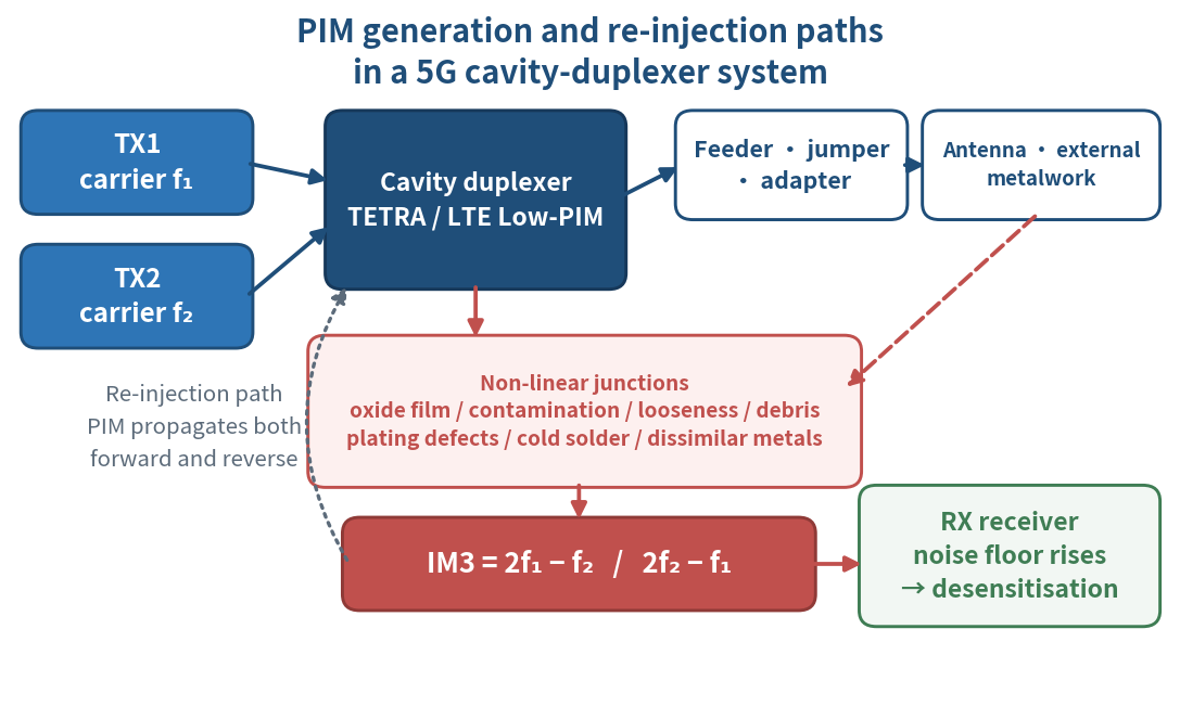
1. Introduction: How PIM Harms Base-Station Operation
1.1 What PIM is, and why it appears in passive components
Passive intermodulation (PIM) refers to unintended frequency components generated when two or more high-power RF signals pass through a passive path that exhibits non-linear behaviour. That passive path covers antennas, feeders, jumpers, connectors, cavity filters, duplexers, diplexers, couplers, surge arresters, terminations and attenuators — in other words, every component along the RF chain that was assumed to be linear.
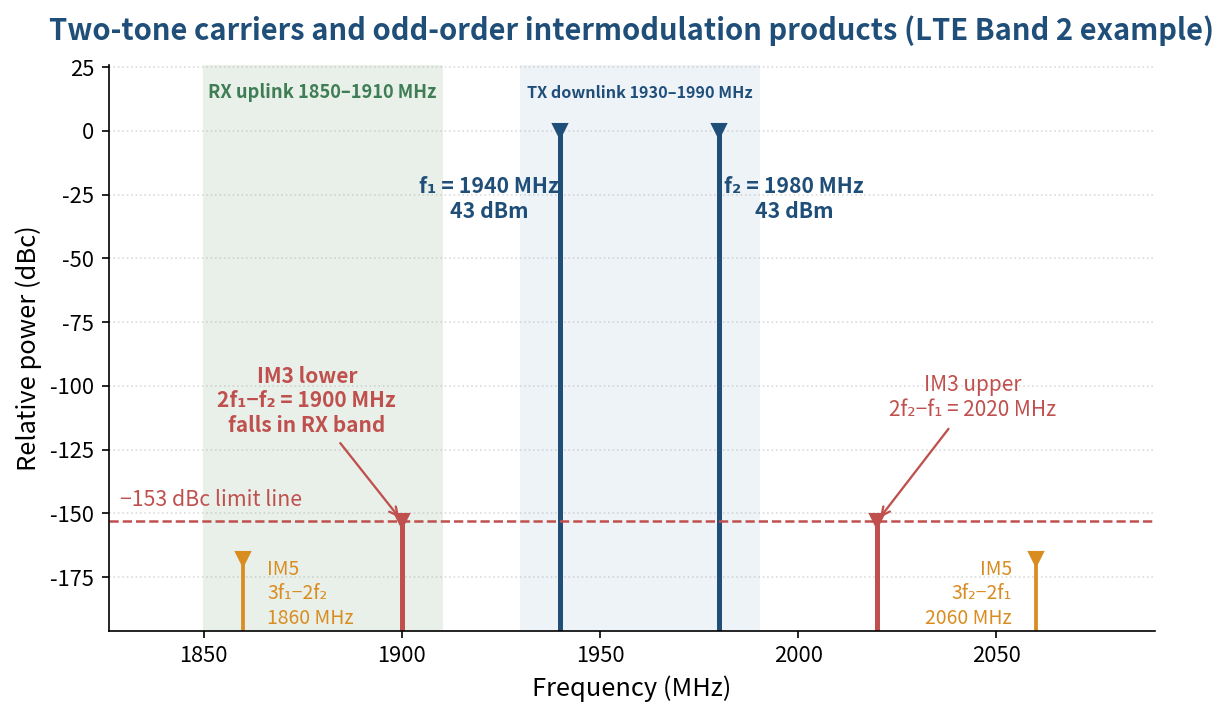
For two carriers f₁ and f₂, intermodulation products appear at every combination m·f₁ ± n·f₂, with order defined as |m| + |n|. Even-order products normally fall far from the carriers and are easily filtered out; the troublesome ones are the odd orders, and third order (IM3) above all, because they sit either side of the carriers separated by the carrier spacing — frequently landing squarely in the same system's receive band.
1.2 Frequency placement: why IM3 is particularly damaging
Take LTE Band 2: the downlink transmit band is 1930–1990 MHz and the uplink receive band 1850–1910 MHz. With two transmit carriers at 1940 MHz and 1980 MHz, the lower third-order product is 2 × 1940 − 1980 = 1900 MHz — squarely inside the station's own uplink receive band. No amount of receive-filter rejection helps here, because the interference is generated on a passive interface downstream of the filter and upstream of the antenna, travelling the same path as the wanted receive signal.
| Order | Product frequency | Relation to carriers | Engineering significance |
|---|---|---|---|
| IM2 | f₁ + f₂ , f₂ − f₁ | Far from the carriers | Usually filterable; still to be checked in multi-band co-siting |
| IM3 | 2f₁ − f₂ , 2f₂ − f₁ | Immediately either side, spaced by the carrier separation | Highest level and most likely to land in the receive band — the principal acceptance metric |
| IM5 | 3f₁ − 2f₂ , 3f₂ − 2f₁ | Twice as far from the carriers as IM3 | Lower in level, but must be swept in systems with wide duplex spacing |
| IM7 | 4f₁ − 3f₂ , 4f₂ − 3f₁ | Three times as far from the carriers as IM3 | Generally negligible, but observable on a severely non-linear junction |
1.3 Quantifying the harm: how much interference does −153 dBc represent?
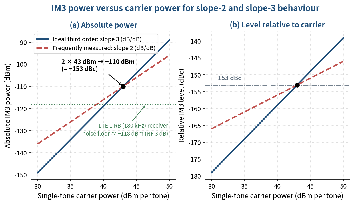
PIM is normally expressed in dBc, relative to the carrier level. Under the standard two-tone condition of 43 dBm (20 W) per tone, −153 dBc corresponds to an absolute power of 43 − 153 = −110 dBm. That number only becomes meaningful against the receiver noise floor: from the thermal-noise power kTB, the noise floor of a single LTE resource block (1 RB, 180 kHz) is about −174 + 10 log₁₀(1.8 × 10⁵) ≈ −121.4 dBm, and with a receiver noise figure of 3 dB the actual floor is about −118.4 dBm.
In other words, a −110 dBm PIM product landing on that resource block sits roughly 8 dB above the noise floor — enough to compress the signal-to-noise ratio of that block appreciably, reduce the usable modulation order and throughput, and, for cell-edge users, show up directly as degraded connection quality and dropped calls. This is exactly why low-PIM specifications are set at such demanding levels: the benchmark is not the transmit power but the receiver noise floor.
1.4 Why PIM risk is higher in 5G macro cells than in earlier generations
- Carrier aggregation, co-siting and shared-antenna architectures greatly increase the number of carrier combinations, each of which can produce an intermodulation frequency inside the receive band.
- Wideband modulation such as OFDM has a high peak-to-average power ratio, so instantaneous peak power far exceeds average power and non-linear defects are more readily excited under real operating conditions.
- Massive MIMO and antenna arrays multiply the number of passive components, junctions and feeders, and with them the number of potential PIM sources.
- Spectrum is increasingly congested, and avoiding every intermodulation frequency by frequency planning alone is no longer feasible.
- Multi-carrier modulated signals produce not a single intermodulation tone but a broadened intermodulation spectrum, so the interference covers more bandwidth than a two-tone CW test would suggest.
1.5 Objectives
The objectives of this study are: (1) to decompose the generation mechanisms of PIM, separating micro-scale contact non-linearity, material and plating defects, and impedance mismatch; (2) to establish the quantitative relationship between return loss, reflection coefficient and VSWR, and to define both the contribution and the limits of matching in controlling PIM; (3) to decompose −153 dBc @ 2 × 43 dBm into a complete, repeatable set of acceptance conditions with a matching measurement procedure; (4) to summarise the real effect of torque, cleanliness and cable restraint during field installation; and (5) to map the immediately deployable engineering capability of Temwell's current cavity duplexer and low-PIM diplexer product lines.
2. PIM Generation: Non-linear Junctions, Material Defects and Impedance Mismatch
2.1 Non-linearity at the micro-contact scale
When two metal surfaces are pressed together, the apparently continuous interface is not flat at microscopic scale. Conduction actually occurs only at a small number of micro-contact spots, whose total area is typically a very small fraction of the nominal contact area. Where the interface carries oxide, contamination films, moisture, flux residue or metal particles, or where contact pressure is insufficient, current is forced through an even smaller area, contact resistance rises, and the resistance itself becomes non-linear with respect to current and temperature.
At high RF power, the local field strength across these tiny regions can be enough to cause electron tunnelling, breakdown or micro-arcing through a thin oxide film. In addition, the high current density over a very small contact area produces localised Joule heating, and metal resistance itself rises with temperature — this electro-thermal coupling makes the resistance vary dynamically within the RF cycle, which is equivalent to a non-linear element. Either mechanism gives the junction diode-like rectifying behaviour, and hence generates intermodulation products.
This also explains the property of PIM that engineers find most troublesome: it is time-dependent and intermittent. Corrosion, loosening, thermal cycling and vibration cause the contact state to vary with time, temperature and humidity, so a junction that measures within specification today may fail after a change of season or a few thermal cycles.
2.2 Material, plating and process defects
A low-PIM structure should be built from non-ferromagnetic, highly conductive materials with a stable manufacturing process. Ferromagnetic materials — nickel, nickel-bearing alloys, nickel underplate, the ferromagnetic phases in stainless steel — exhibit hysteresis, and their magnetisation curve is itself non-linear; they are among the material classes most worth avoiding at the design stage.
One common misconception deserves emphasis: gold plating does not equal low PIM. Soft platings such as gold and silver are valuable because they form a stable, low-resistance, oxidation-resistant contact interface on harder base materials such as brass or beryllium copper. ITU-T K.149 likewise notes that such soft platings must be applied at sufficient thickness over the harder substrate in order to improve interface conduction and contact reliability. But if the underplate can introduce magnetic effects, if the plating is too thin, porous or cracked, if the surface is contaminated, or if contact pressure is wrong, a gold-plated part will still fail PIM.
| PIM type | Where it originates | Typical causes | Who owns the fix |
|---|---|---|---|
| Design PIM | Inside the component structure | Ferromagnetic materials, poor plating design, excessive current density in high-field regions, badly designed mating surfaces | Component design and materials engineering |
| Assembly PIM | Interfaces and junctions | Under- or over-torque, contamination, metal debris, cold solder, scratched plating, foreign objects | Process control and installation SOP |
| External PIM | The environment outside the component | Corroded railings near the antenna, rooftop metalwork, loose bolts, metal-to-metal contact (the “rusty bolt” effect) | Site survey and maintenance |
2.3 The role of impedance mismatch — and its limits
When a duplexer or its external feeder departs from the 50 Ω system impedance, part of the incident power is reflected, and the reflected wave combines with the incident wave to form a standing wave. The standing wave produces periodic voltage and current maxima and minima along the line: the voltage peak can reach (1 + |Γ|) times that of the travelling wave, and the same applies to current. If those peaks coincide with potential non-linear sites — a connector interface, a cavity seam, a tuning screw, a solder joint — the local field and current density there exceed the ideally matched case, and the probability of exciting a non-linearity rises with them.
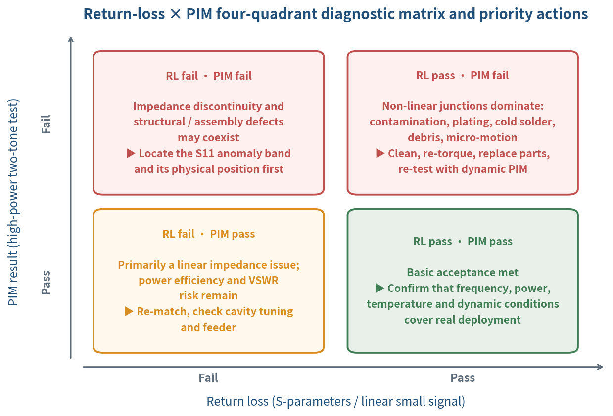
It is important not to reduce this relationship to “better return loss always means lower PIM”. Return loss measures impedance reflection under linear, small-signal (or specified-power) conditions; PIM assesses non-linear behaviour at high power. Good matching is one necessary condition for reducing PIM risk, not a sufficient one — and that is the central engineering issue addressed in Section 4 and Fig. 4.
3. Low-PIM Design Elements: Connector Selection, Soldering and Plating
Low PIM is not a single design parameter but a system property determined jointly by materials, mechanics, surface finish and assembly process. For a 5G cavity duplexer, electromagnetic design, mechanical tolerances, surface treatment and assembly SOP should be treated at the design stage as one exercise in linearity design, rather than as separate pursuits of low insertion loss or high isolation.
3.1 Connector selection
The connector is the interface where mechanical stress concentrates most and which is most often re-mated, making it the first priority in low-PIM design. Selection should confirm: an explicit low-PIM rating (not merely a “gold plated” marking); non-ferromagnetic body and contact springs; a plating stack that has been PIM-verified; adequate contact area and spring contact pressure; and a clearly specified mating torque from the manufacturer.
Equally important is minimising the number of interfaces. Every additional adapter or in-line component adds at least two metal contact surfaces, and therefore two more potential PIM sources. In a low-PIM system, one low-PIM jumper of the correct length is always better than two jumpers plus an adapter made up to length.
3.2 Soldering process
Solder joints are a common PIM source inside cavities and at port transitions. Cold joints, dry joints, micro-cracks and flux residue all create an unstable conductive interface: the intermetallic layer of a cold joint is discontinuous and its conduction varies with temperature and stress, while flux residue forms a conductive or semi-conductive film in the presence of moisture. The soldering process must be controlled through a stable thermal profile, low-residue solder and a reliable cleaning step, evidenced by visual, X-ray or pull testing — and ultimately verified by measured PIM.
Post-thermal-cycling re-testing matters particularly here. Solder joints often fail not at shipment but after tens of temperature cycles, when accumulated thermal stress produces micro-cracks; at that point static PIM may still marginally pass, while a dynamic-disturbance test will expose the problem immediately.
3.3 Gold and silver plating
Plating design must be accepted on four parameters together: thickness, adhesion, porosity and underplate material. Insufficient thickness wears through after mating or thermal cycles; poor adhesion delaminates; porosity lets the base metal corrode in the presence of moisture, and the corrosion product is itself a non-linear medium; and if the underplate is ferromagnetic, hysteresis non-linearity still contributes to PIM through the current path within the skin depth, even with an intact gold surface.
In practice, silver plating is commonly used on cavity interior walls to lower surface resistance and raise unloaded Q, while gold is used at connectors and contact interfaces to secure long-term contact stability and oxidation resistance. Their acceptance criteria differ — conductivity and uniformity for the former, contact reliability and wear resistance for the latter — but both must be confirmed by measured PIM together with salt-spray and damp-heat reliability testing.
3.4 Cavity structure and mechanical stability
Cavity seams, cover screws and tuning screws are the main sources of design PIM. RF current must cross these seams, and if contact pressure is uneven or the seam carries burrs, oxide or machining debris, a non-linear junction forms in a region of high current density. The design should place seams in low-current-density regions where possible, increase screw density to make contact pressure more uniform, and ensure thorough deburring and cleaning after machining.
| Design aspect | Low-PIM principle | Typical failure mode | Verification focus |
|---|---|---|---|
| Connector selection | Low-PIM rating, non-ferromagnetic materials, verified plating, adequate contact area; minimise adapters | Plating damage, incorrect centre-pin depth, under- or over-torque, foreign objects | PIM, S11, mating cycles, torque consistency, visual inspection |
| Cavity and mating surfaces | Keep RF contact surfaces conductive, flat, low in roughness and evenly loaded; control screw layout and seam position | Seam micro-motion, burrs, oxidation, excessive local current density | Dynamic PIM, post-vibration / post-thermal-cycling PIM, sealing and mechanical inspection |
| Soldering | Stable thermal profile, low-residue solder, reliable cleaning; avoid cold joints, dry joints and solder splash | Micro-cracks, flux residue, joint degradation after thermal cycling | X-ray / visual, pull or peel test, PIM, post-thermal-cycling re-test |
| Gold / silver plating | Design thickness, adhesion, porosity and underplate together; avoid ferromagnetic underplate | Thin plating, porosity, cracking, contamination, magnetic underplate effects | Thickness, adhesion, surface analysis, PIM, salt-spray and damp-heat testing |
| Mechanical structure | Keep RF junctions free from cable tension, differential thermal expansion and sustained vibration | Loosening, fatigue cracking, transient PIM under vibration | Restraint fixtures, dynamic PIM, vibration and thermal-cycling testing |
4. How the Matching Network Affects PIM
4.1 Quantifying reflection: reflection coefficient, return loss and VSWR
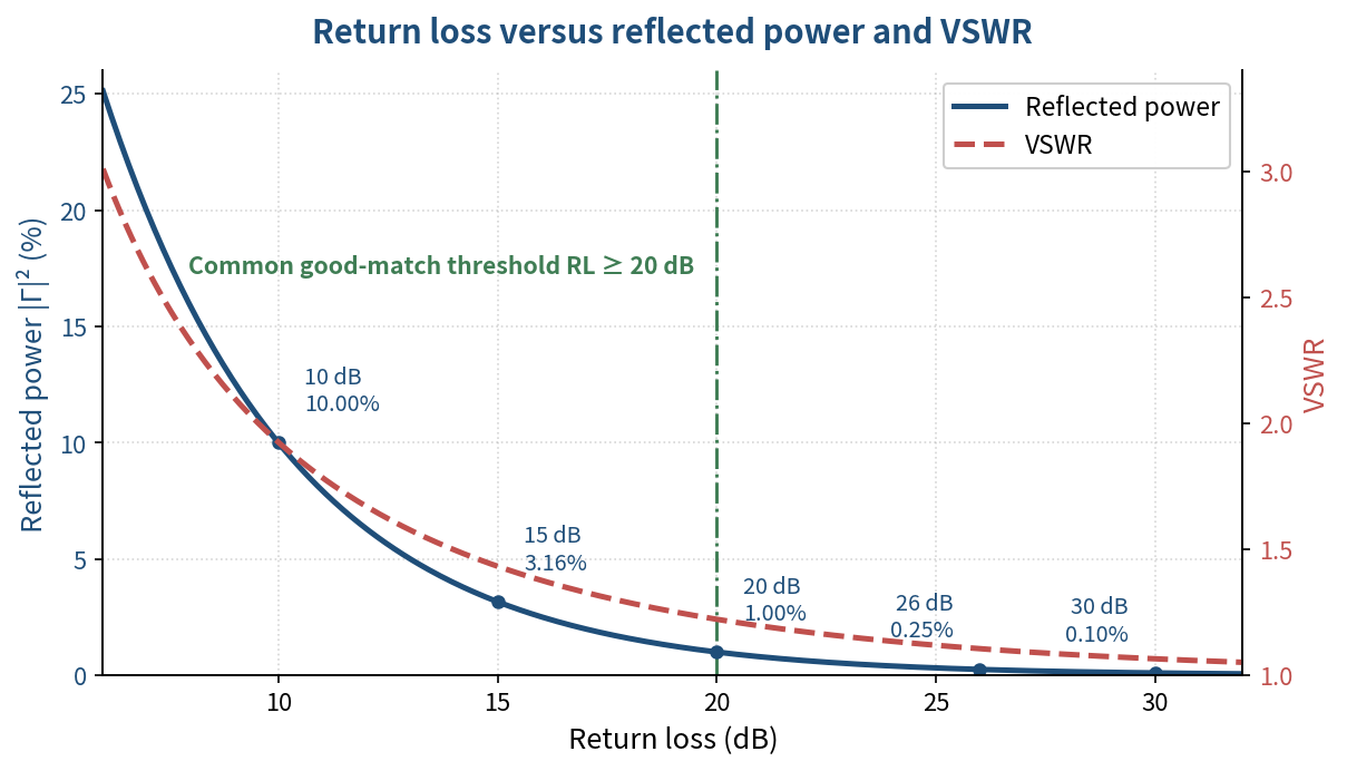
In a 50 Ω system the reflection coefficient between a load impedance Z_L and the characteristic impedance Z₀ is Γ = (Z_L − Z₀)/(Z_L + Z₀). Engineering practice expresses the magnitude of reflection as return loss (RL), related to reflected power ratio and standing-wave ratio by:
| Return loss | Reflection coefficient |Γ| | Reflected power | VSWR | Engineering interpretation |
|---|---|---|---|---|
| 10 dB | 0.316 | 10.00 % | 1.925 | Significant mismatch — check ports, feeder and cavity tuning |
| 15 dB | 0.178 | 3.16 % | 1.433 | Acceptability depends on the system specification; usually still insufficient for a macro site |
| 20 dB | 0.100 | 1.00 % | 1.222 | The common good-match threshold and the baseline of most duplexer specifications |
| 26 dB | 0.050 | 0.25 % | 1.105 | Better match — further reduces standing-wave peaks and local field strength |
| 30 dB | 0.032 | 0.10 % | 1.065 | Approaching the practical limit of measurement and fixturing; diminishing returns |
4.2 How good matching reduces the conditions for exciting PIM
Matching contributes to PIM control along a clear physical chain: lower |Γ| → less reflected wave → lower voltage and current peaks in the standing wave → lower local field and current density at non-linear sites → lower probability of exciting a non-linearity. Comparing RL = 10 dB with RL = 20 dB, |Γ| falls from 0.316 to 0.100 and the voltage peak factor (1 + |Γ|) from 1.316 to 1.100, a reduction of about 16 %; at the same time reflected power falls from 10 % to 1 %, reducing round-trip loss and thermal loading on the feeder.
Every link in that chain is probabilistic rather than deterministic, however. If a non-linear junction happens to sit near a current node of the standing wave, PIM may measure well even with a poor match; conversely, if the junction sits at a current maximum, a contaminated interface will produce severe PIM even at RL = 26 dB. This is the physical root of the relationship between matching and PIM being correlated but not equivalent.
4.3 Three-port matching in a cavity duplexer
A cavity duplexer combines a TX and an RX filter branch at a shared antenna port. Matching design is not simply a matter of tuning the S11 of one branch: it must address reflection at all three ports under their respective operating conditions, together with the load interaction between branches at the common junction — the impedance the RX branch presents across the TX band directly determines the combined load the TX branch sees there.
| Port / item | Design target | Measurement method | Relation to PIM |
|---|---|---|---|
| TX port S11 | RL ≥ 20 dB across the TX passband | VNA with the other ports in precision 50 Ω loads | TX is the high-power path; reflection directly affects standing-wave peaks and local field strength |
| RX port S22 | RL ≥ 20 dB across the RX passband | As above | Affects the receive link budget; reflection alone generates no PIM but does alter the field distribution |
| ANT port S33 | RL ≥ 20 dB across both the TX and RX passbands | As above, then re-checked with the actual jumper and antenna load | The common port carries the full transmit power and is the most critical match point |
| TX→RX isolation | Per system requirement, typically ≥ 60 dB | VNA S21 / S31 | Insufficient isolation lets transmit energy into the receive branch, amplifying the impact of in-band PIM |
| Passband insertion loss | Per part-number specification, TX branch first | VNA S21 | Higher IL means more dissipation in the cavity, raising junction temperature and electro-thermal non-linearity risk |
The recommended matching workflow is: (1) build a full-wave electromagnetic model of the cavity, coupling structures, ports and housing joints, and inspect where the high-field regions lie; (2) taking 50 Ω as the system reference, set return-loss, insertion-loss, isolation and power-handling targets for each port passband; (3) adjust input/output coupling through coupling loops, probe position, iris dimensions, tuning screws or an external low-loss matching section; (4) measure the complete three-port S-parameter set on a VNA; (5) run high-power two-tone PIM on the finished unit in its real jumper configuration, adding dynamic disturbance where required; (6) if PIM fails while the S-parameters are good, investigate junctions, plating, soldering, debris, cable stress and fixture residual PIM first — do not repeatedly re-tune the match.
4.4 The return-loss × PIM diagnostic matrix
The most valuable diagnostic tool in practice is to place the S-parameter result and the PIM result on a single matrix. The four combinations point to different root causes and different priority actions, and the “return loss passes, PIM fails” quadrant is both the most common and the most frequently misdiagnosed — engineers repeatedly re-tune the match there, while the real problem lies in the mechanical interface.
5. Temwell Low-PIM Standard: −153 dBc @ 2 × 43 dBm and Test Methodology
5.1 Decomposing a single number into complete acceptance conditions
“PIM ≤ −153 dBc @ 2 × 43 dBm” is a widely quoted low-PIM statement, but the number alone does not constitute a repeatable acceptance condition. ITU-T K.149 positions −153 dBc @ 2 × 43 dBm as a calibration reference for the measurement system: a standard component of that fixed value, combined with low-PIM loads, is used for cascaded verification, and the result should fall within −153 dBc ± 3 dB. That is a traceability baseline for the measurement system — a different matter from guaranteeing the value for a given finished part number.
| Specification field | What must be stated | Consequence if omitted |
|---|---|---|
| PIM metric and order | For example IM3 ≤ −153 dBc; IM5 and IM7 requirements, if any, listed separately | Results of different orders cannot be compared and the sweep range cannot be defined |
| Excitation conditions | Two-tone CW with f₁ and f₂ each at 43 dBm (20 W); any other power stated explicitly | The dBc figure varies with carrier power, so results at different powers are not comparable |
| Measurement mode | Reflected or transmitted, stated explicitly | The two modes measure PIM on different paths and can differ by several dB |
| Measurement band | Specified TX tone frequencies, IM3 sweep range and the RX bands they may fall into | There is no way to confirm that the worst-case placement was covered |
| DUT condition | Port terminations, connector types, mating torque, jumpers, fixture and tuning state | The same unit can measure more than 10 dB apart in different fixtures |
| Dynamic conditions | Whether vibration, tapping or gentle cable flexing is applied, and the pass/fail logic | Intermittent PIM defects escape detection and appear only in the field |
| Environmental conditions | Temperature, humidity, warm-up time, and whether the test follows thermal cycling or burn-in | Contact PIM varies with temperature; passing at ambient does not mean passing across the full range |
| Uncertainty | Instrument residual PIM, standard-component verification result, repeatability and guard band | It cannot be determined whether the reading reflects product performance or the measurement system's noise floor |
5.2 Power slope: why the figure cannot be extrapolated to other powers
The absolute power of a third-order product theoretically follows a 3:1 slope against carrier power: each 1 dB of carrier increase raises absolute IM3 by 3 dB, so the carrier-referenced dBc figure degrades by 2 dB. In measurement, the slope of contact PIM often lies between 2 and 3, because electro-thermal effects and the contact state itself change with power rather than following an ideal third-order polynomial. Whatever the slope, the conclusion is the same: a dBc figure measured at 2 × 43 dBm cannot be used to guarantee behaviour at higher power.
5.3 The six-stage measurement procedure
- Establish the test-chain baseline. Replace the DUT with low-PIM loads and measure the residual PIM of the complete system. The residual should be clearly below the DUT target — at least 10 dB is recommended — otherwise the measurement reflects the system rather than the product.
- Verify the two-tone power. Confirm the actual power of f₁ and f₂ at the DUT input with a power meter, recording the losses of cables, couplers, filters and adapters, so that the instrument setting is not mistaken for the power actually delivered.
- VNA pre-check. Measure the three-port S-parameters, return loss, insertion loss and isolation first, confirming there is no gross mismatch or assembly error. Any S-parameter anomaly should be cleared before high-power testing begins.
- Static PIM test. Measure IM3 according to the specified f₁, f₂ and sweep plan, and calculate whether 2f₁−f₂ and 2f₂−f₁ fall into the receive band. The worst-case frequency combinations across the passband must be covered, not a single spot frequency.
- Dynamic PIM test. Without damaging the unit, apply controlled gentle disturbance — tapping, slight flexing, vibration — to mating interfaces, mounting structure and cables to expose defects sensitive to micro-motion or stress. This step is the only effective way to intercept intermittent PIM.
- Repeatability and traceability. Record test frequencies, power, temperature, torque, fixture, serial number, operator and raw traces. Where a result is close to the limit, re-mate and re-measure several times and retain the spread as the basis for a guard-band decision.
To be confirmed: the formal datasheets, specified bands, port types and customer acceptance conditions of the current Temwell TETRA Cavity Duplexer and LTE Low PIM Diplexer part numbers are not contained in the public material cited here. This paper therefore presents a recommended specification and measurement framework, and must not be used as a guaranteed figure for any specific model; formal part numbers and datasheet values should be supplied by the product department before external publication.
6. Field Installation: Mating Torque and Connector Cleanliness
PIM failures in the field are frequently caused not by the duplexer's filter response but by what sits either side of it: jumpers, adapters, the antenna port, surge arresters, grounding hardware, or corroded metalwork near the antenna. A duplexer that passed at the factory can be degraded past specification within minutes by incorrect installation practice — and that degradation is irreversible, because plating crushed or scraped away by over-torque cannot be restored.
6.1 Mating torque
The effect of torque on PIM degrades on both sides of the optimum. Under-torque gives insufficient contact pressure, so conduction occurs at only a few micro-contact spots; contact resistance is high and vibration-sensitive, producing intermittent PIM. Over-torque deforms the interface plastically, damages plating, wears the thread and generates metal debris — and that debris is itself a fresh PIM source. Minimum PIM occurs within the manufacturer's specified torque window, not at “as tight as possible”.
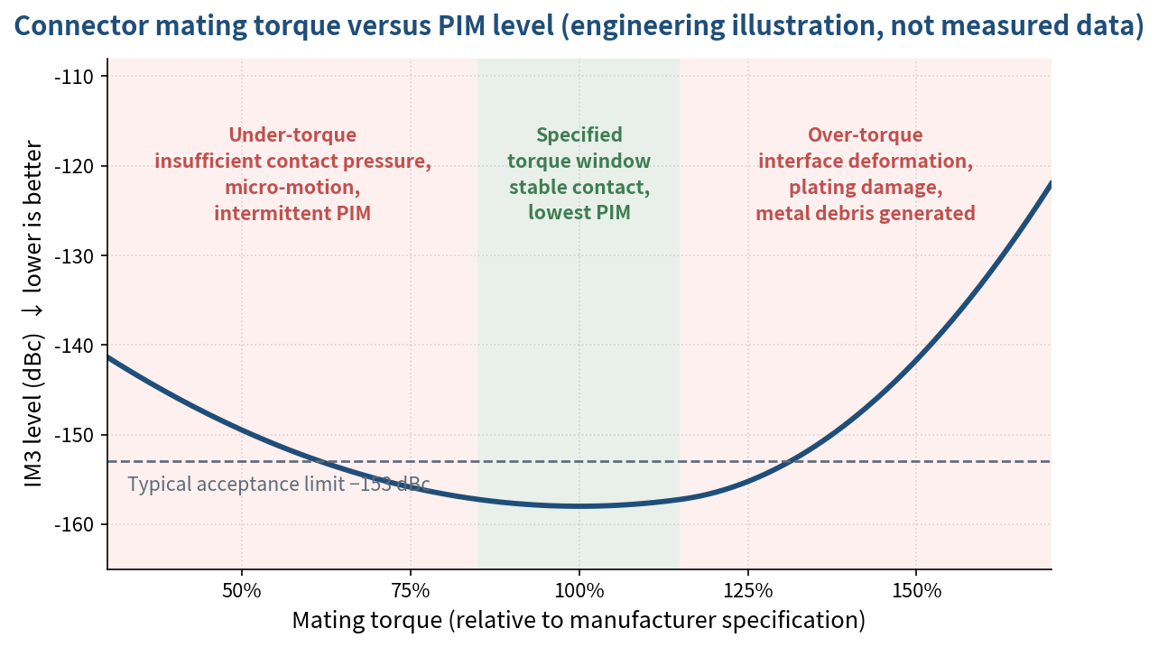
Three practical requirements follow: use a calibrated torque wrench, not an ordinary spanner or hand tightening; follow the connector manufacturer's specified torque exactly, since it differs between models and platings; and when mating, rotate only the coupling nut, never the two bodies relative to one another — relative rotation scrapes the contact surfaces, generating wear particles and damaging the plating at the same time.
6.2 Interface inspection and cleaning
Every interface should be inspected visually before mating: contamination, metal debris, burrs, scratches, dents, plating damage and incorrect centre-pin depth. Cleaning must follow the connector manufacturer's procedure using lint-free, residue-free methods; the wrong technique — blowing compressed air into the interface, or using a wiping material that sheds fibres — can push foreign matter deeper into the interface and create a worse problem than the one being solved.
6.3 Cable restraint, weatherproofing and external PIM sources
Jumpers must be properly restrained against sustained tension, tight bends and long-term vibration — all of these stresses ultimately reach the connector contact interface and cause fretting wear and fatigue. Weatherproofing determines long-term behaviour: once moisture or salt spray enters an interface, corrosion products form a non-linear film within months and a previously compliant junction degrades progressively. Sealing integrity must be restored after any maintenance work, a point frequently overlooked in practice.
Finally, there is the environment beyond the components. Corroded railings near the antenna, rooftop metal sheets, loose bolts and brackets can all form metal–oxide–metal contacts under strong RF fields, generating intermodulation that is re-radiated back into the antenna — the “rusty bolt” effect. No duplexer replacement fixes this; it must be located and removed through site survey and distance-to-PIM style measurements.
| Item | Installation requirement | PIM significance |
|---|---|---|
| Interface inspection | Check for contamination, metal debris, burrs, scratches, dents and plating damage before mating | Prevents local field concentration and non-linear contact points |
| Cleaning | Clean per the connector manufacturer's procedure using lint-free, residue-free methods; do not push debris into the interface | Reduces intermittent PIM caused by contamination films and loose particles |
| Torque | Use a calibrated torque wrench and follow the manufacturer's specified value exactly | Insufficient pressure produces PIM; over-torque deforms, wears and generates debris |
| Connector rotation | Rotate only the coupling nut; never rotate the two bodies against each other | Reduces wear particles and damage to the centre contact and plating |
| Number of interfaces | Remove unnecessary adapters and in-line components; use jumpers of the correct length | Every additional metal contact surface adds another potential PIM source |
| Cable restraint | Secure jumpers against tension, tight bends, sustained vibration and moisture ingress | Prevents fretting, fatigue and environment-dependent PIM at the contact interface |
| Weatherproofing | Apply appropriate weatherproofing and restore sealing integrity after every maintenance action | Reduces long-term degradation from moisture, salt spray and oxidation |
| External environment | Inspect corroded railings, rooftop metalwork, bolts and loose brackets near the antenna | Guards against re-radiated “rusty bolt” PIM originating outside the antenna |
7. Conclusions: Best Practice for a Low-PIM Filter System
7.1 Conclusions
- Conclusion 1: PIM and matching must be accepted separately and optimised together.Return loss / S11 is the key metric for 50 Ω matching and reflection control; PIM is the metric for high-power non-linearity. They are correlated but not equivalent, and both VNA S-parameter data and high-power two-tone PIM data are required for product and system acceptance.
- Conclusion 2: every RF contact surface is within the scope of low-PIM design.Cavity seams, tuning structures, connectors, jumpers, solder joints, plating, adapters and mounting brackets can each be the dominant PIM source. Improving the filter circuit without controlling mechanical interfaces will not deliver stable low PIM.
- Conclusion 3: −153 dBc @ 2 × 43 dBm must be stated with its full conditions.Without the test band, IM order and placement, measurement mode, ports and fixture, torque, dynamic conditions, environment and uncertainty, the number is not comparable between laboratories or sites. ITU-T K.149 positions it as a calibration reference for a standard component, not as a universal product guarantee.
- Conclusion 4: a dBc figure cannot be extrapolated across power levels.Under ideal third-order behaviour each 1 dB of carrier increase degrades the dBc value by 2 dB, and measured slopes commonly lie between 2 and 3. The acceptance power must reflect the real operating condition.
- Conclusion 5: low PIM is a closed loop across design, manufacturing, installation and maintenance.Design controls materials, field strength and impedance; manufacturing controls plating, soldering and cleanliness; installation controls torque, cleaning and cable restraint; maintenance establishes traceable procedures using PIM, VNA and external-source investigation. If any one link is out of control, the investment in all the others is cancelled out.
7.2 Mapping to Temwell's immediately deployable capability
Building on more than 25 years of RF filter manufacturing experience, Temwell Corporation has directly applicable engineering capability in the following five areas, which translate immediately into low-PIM cavity duplexer products and services:
| Engineering capability | Corresponding technology / product line | Deliverable customer value |
|---|---|---|
| Duplexer and multiplexer integration | TETRA Cavity Duplexer, LTE Low PIM Diplexer, cavity quadplexers; three-port matching and isolation co-designed | One-stop integrated delivery for multi-band co-siting and carrier aggregation |
| Low-PIM materials and surface finishing | Non-ferromagnetic material selection, controlled silver/gold plating (thickness, adhesion, porosity, underplate) | Design PIM reduced at the material stage rather than screened out afterwards |
| Precision mechanics and assembly process control | Seam pressure layout, deburring and cleanliness control, torque and fixture SOPs, key process characteristic (KPC) management | Lower batch-to-batch variation in assembly PIM, with better yield and consistency |
| Dual-track S-parameter and PIM acceptance | Full three-port VNA measurement plus high-power two-tone PIM including dynamic disturbance; serialised raw traces retained | Traceable shipping reports that support dispute resolution at the customer and in the field |
| Customisation and short lead time | Centre frequency, bandwidth, isolation, power, connector type and mechanical dimensions all customisable, with a 7–10 day standard lead time | Serves 5G, public-safety, aerospace, defence and satellite applications |
7.3 Twelve-month development roadmap
- Build a complete PIM / IL / RL / isolation / power / environment specification matrix for every TETRA Cavity Duplexer and LTE Low PIM Diplexer part number, and incorporate it into the formal datasheets.
- Establish a residual-PIM traceability procedure for the internal low-PIM measurement system, covering standard-component verification intervals, low-PIM load management and uncertainty assessment.
- Bring dynamic-disturbance PIM testing into the standard shipping flow with quantified pass/fail logic (a level-variation threshold during disturbance).
- Build a process database linking plating combinations (thickness, underplate, porosity) to measured PIM results, as the material-selection basis for new part numbers.
- Develop a customer installation support package — low-PIM jumper recommendations, torque specification cards, installation checklists and field investigation procedures — to reduce post-shipment PIM disputes in the field.
Temwell is headquartered in Taipei, Taiwan, with more than 25 years of RF filter development and manufacturing experience and partners in over 20 countries across the Americas, Japan, Europe and Australia. Its product ecosystem spans cavity, helical, SMD ceramic and SAW filters together with diplexers, duplexers and multiplexers, extended through the Temstron brand into RF amplifiers and active and passive components. As 5G macro cells, public-safety private networks and multi-band co-siting place ever more demanding requirements on linearity, the system-level low-PIM control framework presented here maps directly onto Temwell's current design, process and measurement capability, with customised delivery in a 7–10 day lead time.
Appendix - Complete source FAQ
FAQ — Low-PIM Matching Techniques for 5G Cavity Duplexers in Macro Cell Applications (A-10)
This FAQ is compiled from the PIM generation model, Tables 1–8 and Figures 1–6 of this paper (Article No. A-10). Unless otherwise stated, the values quoted are theoretical calculations, public standards and test-instrument vendor technical material, together with Temwell process and measurement experience — not the measurement report of a single finished unit. Actual product specifications are governed by the formal datasheet and shipping test report of each part number.
Category 1 — Technical specification and design
-
What frequency bands and bandwidths does this filter design mainly support?
This paper addresses cavity duplexers and low-PIM diplexers covering TETRA private-network bands (typically 350–470 MHz) and LTE/5G Sub-6 GHz macro-cell bands (typically 700 MHz–3.8 GHz). The spectral placement calculations in the text use LTE Band 2 (TX 1930–1990 MHz, RX 1850–1910 MHz) as the worked example. For a duplexer, bandwidth must be quoted separately for the TX and RX branches, together with the duplex spacing and the transition-band width — these three items jointly bound the achievable isolation.
-
What are the rated power and impedance conditions of this filter?
System impedance is 50 Ω. The low-PIM acceptance baseline used here is the standard two-tone condition of 43 dBm (20 W) per tone, 40 W total. Note that rated power and PIM test power are different things: expressed in dBc, PIM degrades as carrier power rises — per Fig. 5, under ideal third-order behaviour every 1 dB of carrier increase degrades the IM3 dBc figure by 2 dB. If the actual per-carrier power at a macro site exceeds 43 dBm, the dBc figure obtained at 2 × 43 dBm cannot be carried over directly.
-
Under what measurement conditions were the insertion loss and return loss presented in this paper
obtained?
The return-loss / reflected-power relationships in this paper (Fig. 3, Table 4) are theoretical curves converted directly from RL = −20 log₁₀|Γ| and |Γ|² = 10^(−RL/10); they are not the measurement of a single finished unit. In practice, S-parameters should be measured on a vector network analyser after SOLT/TRL calibration with all three ports terminated in precision 50 Ω loads, while PIM must be measured separately on a high-power two-tone system. The fixture, torque and cable configuration must be recorded in both reports, otherwise the data cannot be compared between laboratories.
-
What are the main advantages of this structure compared with conventional designs such as PCB filters
or SAW/BAW?
A metal cavity is currently the only duplexing structure that simultaneously meets tens-of-watts power handling and −150 dBc-class linearity. SAW/BAW devices generally handle less than a watt, and their piezoelectric material and micro-electrodes are themselves non-linear sources at high power. Planar PCB filters are limited by substrate dielectric loss, very thin conductors and numerous solder joints, making low insertion loss and low PIM hard to achieve together. The metal cavity stores energy in air and spreads current over a large metal surface, so current density per unit area is low and the probability of exciting a non-linearity drops accordingly.
-
Under what conditions does the performance of this design degrade noticeably?
The classic failure mode is a design that is electrically sound but mechanically out of control. The cavity's S-parameters may meet specification completely, yet insufficient connector torque, metal debris left on the interface, porous or cracked plating, a cold solder joint, or a jumper under sustained tension and vibration will degrade PIM by more than ten dB at high power — often intermittently, so the unit passes a static measurement and fails as soon as the cable is tapped or bent. This is precisely why this paper insists that PIM and return loss be accepted as separate tests.
Category 2 — Application scenarios and product selection
-
Which equipment or applications is this filter best suited to?
It suits any high-power scenario in which one antenna must transmit and receive simultaneously: 5G/LTE macro cells, TETRA and P25 public-safety base stations, multi-band co-siting and carrier-aggregation shared-feeder architectures, vehicular and shipborne repeaters, and combining nodes in distributed antenna systems. What these share is high transmit power, demanding receive sensitivity, and only a duplexer separating TX from RX — so any passive non-linearity falls straight back into the station's own receiver.
-
If I need a narrower or wider bandwidth, how can this design be adjusted?
Bandwidth changes in a duplexer must be considered together with isolation and insertion loss. Widening the passband compresses the transition band and lowers TX-to-RX isolation, letting more transmit energy leak into the receive branch. Narrowing it raises stored energy and local field strength inside the cavity, which increases the risk of exciting PIM near tuning screws and mating surfaces. The practical approach is to fix the isolation and PIM targets first, then buy the required bandwidth by adding resonators or introducing transmission zeros — not simply by enlarging the coupling iris.
-
Are there additional requirements or limitations at high power or high temperature?
Three additional requirements. First, the PIM acceptance power must reflect real operating conditions — a result at 2 × 43 dBm cannot be used to guarantee behaviour at 2 × 46 dBm (see Fig. 5). Second, thermal cycling produces relative displacement between metal interfaces with different expansion coefficients, and this is the principal reason contact PIM degrades over time; for high-temperature or outdoor projects a post-thermal-cycling PIM re-test is recommended. Third, multi-carrier and OFDM modulation broaden the intermodulation spectrum, so a plain two-tone CW test may understate real interference; where necessary, verify at system level with the actual modulated signal.
-
For space-constrained designs, how much volume or installation space should be reserved?
The volume of a cavity duplexer is driven mainly by frequency band and required isolation: the lower the frequency and the higher the isolation, the more and larger the resonators. In low-PIM projects, however, the real space constraint is usually not the body but the connector surroundings — clearance for a torque wrench to swing, the minimum bend radius of the jumper, and a routing path that keeps the cable from being continuously stressed by the enclosure. Forcing a jumper into a tight bend or stacking adapters to make a unit fit typically costs more in PIM than the volume saved is worth.
Category 3 — Customisation and engagement process
-
What specification data should be prepared to customise a similar filter?
Beyond the basics — TX/RX passbands, duplex spacing, insertion-loss limit, per-port return loss, isolation and system impedance — a low-PIM project needs five further items: (1) the PIM limit with its complete test conditions (tone frequencies, power per tone, reflected or transmitted method, IM order, sweep range); (2) the actual carrier plan and which IM frequencies may fall in the receive band; (3) connector type, specified torque and field jumper specification; (4) environmental grade (temperature range, ingress protection, salt spray, vibration); (5) whether dynamic-disturbance testing is required and by what pass/fail logic. The full checklist is given in Table 6.
-
How long does it take from specification sign-off to the first samples?
Temwell's standard lead time for customised cavity products is 7–10 days. For low-PIM projects requiring a full PIM test report, verification time must be added: residual-PIM verification of the test chain, static swept PIM and dynamic-disturbance testing typically need one to two working days together. If post-thermal-cycling or post-vibration re-testing is also required, that is timed separately according to the test conditions. It is worth separating the delivery schedule from the verification-report schedule at the quotation stage.
-
What reliability or qualification testing is performed before volume production?
The six-stage procedure of Section 5 is followed: (1) verify the residual PIM of the test chain with low-PIM loads; (2) verify the actual two-tone input power at the DUT with a power meter; (3) VNA pre-check of all three ports (S11/S22/S33, insertion loss, isolation); (4) static swept two-tone PIM, confirming whether IM3 falls in the receive band; (5) dynamic-disturbance PIM on junctions, cables and mounting structure; (6) where required, re-test after thermal cycling, vibration and damp heat. All raw traces, fixture configurations, torque values and serial numbers are kept as traceable records.
-
If an existing design does not fully meet the requirement, what adjustments or evaluation support can
you provide?
Adjustment is possible at three levels. Material and surface: change the plating stack, adjust plating thickness and porosity control, switch to non-ferromagnetic contact parts. Structural: reposition coupling structures and tuning elements to reduce current density in high-field regions, improve the contact pressure and consistency of cavity seams, and remove unnecessary interfaces. System: review the customer's feeder, jumper, surge-arrester and adapter configuration together with the field installation SOP — most field PIM problems originate not in the duplexer body but in the interfaces on either side of it.
Category 4 — Supplementary questions
-
[Supplementary] Does a passing return loss mean PIM will also pass?
No. Return loss measures impedance reflection under linear, small-signal conditions, while PIM assesses non-linear behaviour at high power; the two are related but independent metrics. Good matching lowers reflected power and local standing-wave peaks and therefore reduces the conditions under which a non-linear junction is excited — it is a necessary condition for low PIM risk, but not a sufficient one. The four-quadrant matrix in Fig. 4 exists precisely to handle the most common and most misread combination: return loss passes, PIM fails.
-
[Supplementary] Does gold plating by itself mean low PIM?
It does not. Soft platings such as gold and silver are valuable because they form a stable, low-resistance, oxidation-resistant contact interface on harder base materials such as brass or beryllium copper — not because the plating material itself carries a low-PIM property. If the underplate can introduce magnetic or non-linear effects, if the plating is too thin, porous or cracked, if the surface is contaminated, or if contact pressure is wrong, a gold-plated part will still fail PIM. Plating must be accepted on thickness, adhesion, porosity and measured PIM together.
-
[Supplementary] Can a datasheet figure of “−153 dBc” be compared directly across part numbers and
sites?
Not advisable. A figure of −153 dBc is comparable only when it carries its full conditions: tone frequencies, power per tone, reflected or transmitted method, IM order and sweep range, port terminations and fixture, torque, temperature, plus the residual PIM and uncertainty of the measurement system. ITU-T K.149 positions −153 dBc @ 2 × 43 dBm as a calibration reference point for a standard component (verification results should fall within ±3 dB) — a traceability baseline for the measurement system, not a guaranteed value for any finished part number. Table 6 lists the complete set of specification fields.
References
- ITU-T Recommendation K.149, "Passive intermodulation test methods of array antenna systems in mobile communication systems," approved December 2020, published 2021.
- IEC 62037 series, "Passive RF and microwave devices, intermodulation level measurement," International Electrotechnical Commission.
- Anritsu Company, "Passive Intermodulation (PIM) — Measurement Fundamentals and Field Testing," technical resource, accessed September 2026.
- Analog Devices, "Passive Intermodulation (PIM) Effects in Base Stations: Understanding the Challenges and Solutions," technical article, accessed September 2026.
- Radiall, "Intermodulation Guide," public technical document, accessed September 2026.
- 3GPP TS 38.104, "NR; Base Station (BS) Radio Transmission and Reception," Release 17 / 18.
- 3GPP TS 36.104, "E-UTRA; Base Station (BS) Radio Transmission and Reception," (LTE Band 2 frequency allocation reference).
- ETSI EN 300 392 series, "Terrestrial Trunked Radio (TETRA); Voice plus Data (V+D)," (TETRA band and duplex spacing reference).
- Temwell Corporation, "TETRA Cavity Duplexer / LTE Low PIM Diplexer — Product Catalog & Technical Datasheets," https://www.temwell.com, 2026.
- Project Document: Temwell Website Technical Article Series — Complete Outline of 50 Articles, A-10 Topic, Key Metrics, and Corresponding Products; Publication Schedule for 50 Technical Articles on the Official Website, Article No. 10, Publication Date: September 7, 2026.