

Improving Return Loss of Standard Cavity Bandpass Filters Using Advanced Tuning Structures
Return Loss (RL) is the core metric for the impedance-matching quality of a cavity bandpass filter (CBF); it directly governs the power-transfer efficiency of the RF front end, power-amplifier stability, and receiver noise figure. Taking the TEMWELL Standard Cavity Bandpass Filter as its subject, this paper examines the complete engineering chain for improving RL: from the physical definition of return loss (conversion among S11, VSWR, and mismatch loss), to the key factors affecting RL (input/output coupling structure and resonant-cavity dimensional tolerances), and on to advanced tuning techniques centered on tuning screws and coupling apertures. The TEMWELL factory tuning SOP and RL acceptance criteria are presented, and a 6-pole, 3.5 GHz coaxial cavity filter is used as a worked case: the worst in-band RL improves from 11.3 dB to 21.4 dB (a 10.1 dB gain) while insertion loss drops from 0.72 dB to 0.48 dB.
1. Introduction: Importance of Return Loss to System Matching and Noise
In modern wireless front-end design, the impedance-matching quality of a filter directly determines the power-transfer efficiency and noise behavior of the entire signal chain. Return Loss (RL) is the core metric for that match. When the filter input/output impedance is mismatched to the system reference impedance (typically 50 Ω), part of the incident power returns as a reflected wave, with two serious consequences:
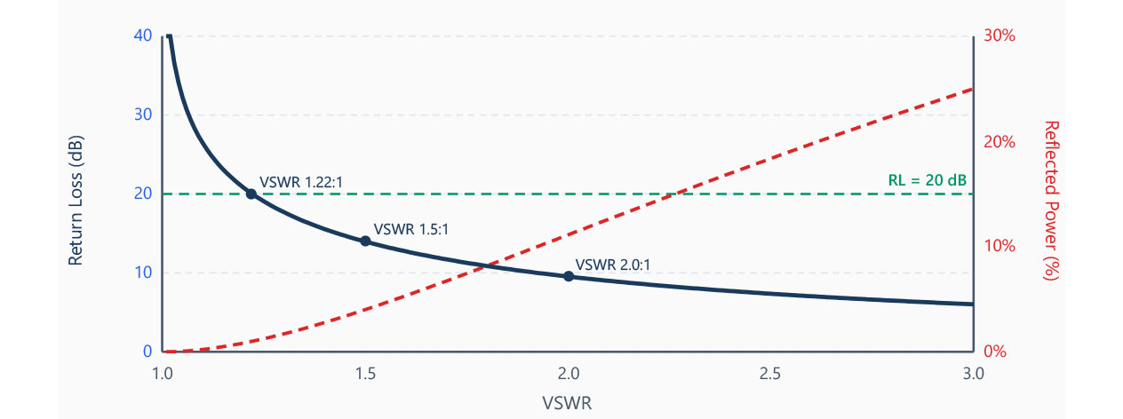
Power loss: the power not delivered to the load is dissipated as a reflected wave, termed mismatch loss. For VSWR = 2:1 (RL ≈ 9.5 dB), the mismatch loss reaches 0.51 dB — roughly 11% of incident power is reflected. For a base-station power amplifier (PA), this can cause instability or even damage.
Noise-figure degradation: in the receive chain, mismatch directly affects the noise figure (NF) of the following low-noise amplifier (LNA). The mismatch loss adds to the LNA NF, reducing sensitivity. For an LNA with NF = 0.5 dB, a front-end filter at VSWR = 2:1 can degrade system NF to ~1.0 dB. For noise-sensitive applications (satellite, radio astronomy), an input VSWR < 1.5:1 is recommended.
Good matching maximizes power transfer, suppresses standing-wave interference, and maintains stable group delay. High-quality cavity bandpass filters therefore require RL ≥ 20 dB (VSWR ≤ 1.22:1) across the full passband — the industry high-grade standard.
2.1 Basic Definitions
Return loss is the ratio of incident to reflected power, in dB:
where Γ (reflection coefficient) is the complex voltage reflection coefficient set by the impedance mismatch:
Z_L is the load impedance and Z₀ the system characteristic impedance (50 Ω). S11 measured by a VNA is exactly this coefficient; in dB, S11 = 20·log₁₀(|Γ|) = −RL, so S11 = −20 dB equals RL = 20 dB.
2.2 Conversion Relationships
The standing-wave ratio is VSWR = (1 + |Γ|) / (1 − |Γ|). Table 1 summarizes the correspondence; Figure 1 plots VSWR versus RL and reflected power.
| VSWR | Reflection |Γ| | Return Loss (dB) | Reflected Power (%) | Mismatch Loss (dB) |
|---|---|---|---|---|
| 1.00:1 | 0.000 | ∞ | 0.0% | 0.00 |
| 1.10:1 | 0.048 | 26.4 | 0.23% | 0.01 |
| 1.22:1 | 0.100 | 20.0 | 1.0% | 0.04 |
| 1.50:1 | 0.200 | 14.0 | 4.0% | 0.18 |
| 2.00:1 | 0.333 | 9.5 | 11.1% | 0.51 |
| 3.00:1 | 0.500 | 6.0 | 25.0% | 1.25 |
2.3 Engineering Significance
Improving RL from 14 dB to 20 dB lowers VSWR from 1.5:1 to 1.22:1 and mismatch loss from 0.18 dB to 0.04 dB. For high-power applications (> 10 W), every 0.1 dB of mismatch-loss improvement directly raises system efficiency and component life.
3. Factors Affecting Return Loss
3.1 Input/Output Coupling Structure
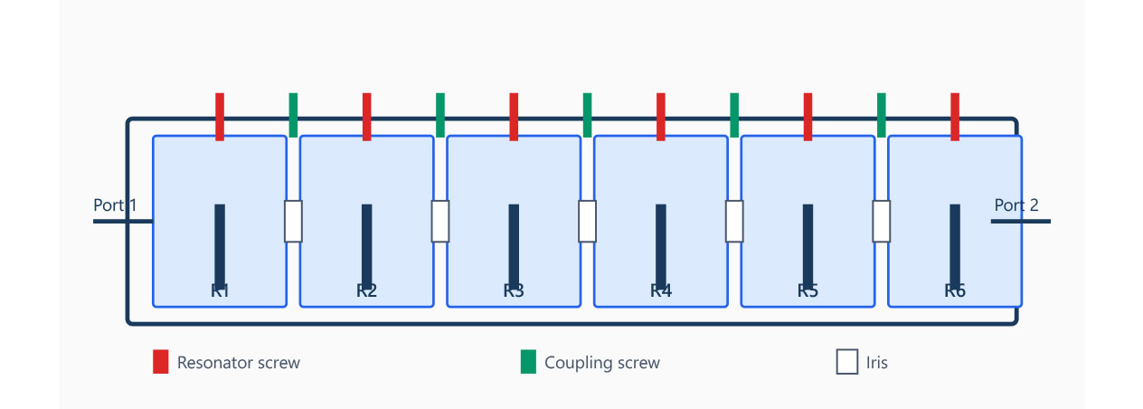
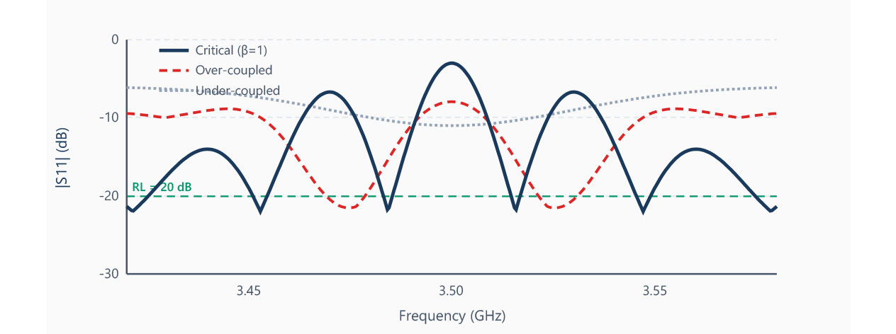
The input/output coupling structure is the most critical element governing RL. Figure 2 shows a 6-pole coaxial cavity BPF with resonator tuning screws, inter-cavity coupling screws, and coupling apertures (irises). The coupling factor is β = Q_u / Q_e, with Q_u the unloaded and Q_e the external quality factor. Table 2 lists the three coupling states; Figure 3 shows the corresponding S11.
| Coupling State | Condition | S11 @ Center | RL Level |
|---|---|---|---|
| Critical | β = 1 | theoretically −∞ dB | Best |
| Over-coupled | β > 1 | double hump in passband | Degraded |
| Under-coupled | β < 1 | S11 rises at center | Worst |
The coupling loop is the most common I/O mechanism in coaxial cavity filters; a larger loop closer to the center post gives stronger coupling (lower Q_e). Rotating the loop angle precisely sets Q_e. The coupling aperture provides inter-cavity coupling — aperture area sets inductive coupling while a screw adds a capacitive trim.
3.2 Resonant-Cavity Dimensional Tolerances
Manufacturing tolerance is a main reason measured RL deviates from design:
- Cavity length: directly affects resonant frequency; ±50 µm yields ~5–10 MHz shift at 3.5 GHz, creating asymmetric S11 ripple.
- Cavity width/depth: affects characteristic impedance and unloaded Q (Q_u).
- Aperture machining: ±0.1 mm² changes adjacent coupling by 5–10%, shifting bandwidth and degrading RL.
- Center-post diameter: affects each cavity frequency — a primary source of in-band ripple.
- Screw-hole position: sets tuning-screw sensitivity and travel range.
Studies show that once waveguide-BPF manufacturing deviation exceeds ±11 µm, the 3 dB maximum allowable RL degradation may be exceeded. Precision factory tuning is therefore necessary to compensate tolerance and ensure RL compliance.
4. Advanced Tuning: Tuning Screws and Coupling Apertures
4.1 Tuning Equipment Setup
Required equipment: a VNA with time-domain capability (e.g. Keysight PNA/ENA), a 50 Ω termination, a SOLT calibration kit, and a non-metallic screwdriver. The VNA should display four traces simultaneously: S11 LOGMAG, S21 LOGMAG, S11 Smith Chart, and S11 Time Domain.
4.2 Tuning-Screw Fine-Tuning Method
A tuning screw adjusts each cavity resonant frequency: deeper insertion increases equivalent capacitance and lowers frequency; withdrawal does the reverse. Table 3 lists the identification method.
| Screw Type | Characteristic Response When Turned |
|---|---|
| Resonator tuning screw | S21 peak shifts left/right; S11 time-domain cavity nulls move |
| Inter-cavity coupling screw | Passband bandwidth/ripple changes; S21 center barely moves |
| I/O coupling screw | S11 depth and Smith-chart position change greatly; S21 shape changes slightly |
Resonator sequential-tuning procedure:
- Set the VNA to time domain and observe the per-cavity S11 reflection nulls (dips).
- From the input (Port 1) side, tune cavities 1…N/2 so each null aligns to the target frequency.
- Switch to S22 and symmetrically tune the remaining cavities from Port 2.
- Return to frequency domain; confirm the S11 ripple count equals the filter order (N equal troughs).
- Fine-tune until ripples are equal in height and symmetric about center.
4.3 Coupling-Aperture Fine-Tuning Method
The coupling aperture and its screw set the inter-cavity coupling (and thus bandwidth and RL ripple height). Deeper insertion strengthens inductive coupling and widens the band; withdrawal narrows it.
Guidelines for adjusting RL:
- Unequal ripple heights indicate a coupling deviation between the corresponding cavities.
- Identify the deepest (best RL) and shallowest (worst RL) ripples.
- Adjust the coupling screw above the corresponding middle (even) cavity to equalize ripple heights.
- If RL is low overall (S11 ≥ −15 dB), check the I/O loop angle to verify β is near critical coupling.
I/O loop fine-tuning: larger projected area (perpendicular to B-field) → lower Q_e → stronger coupling → deeper S11; otherwise S11 rises.
5. TEMWELL Tuning Process: Factory SOP and RL Acceptance
5.1 TEMWELL Standard Cavity BPF Specifications
The TEMWELL Standard Cavity BPF covers 500 MHz–28 GHz, up to 200 W, 50 Ω. Table 4 lists representative specs.
| Model | Center Freq. | Passband | IL | VSWR | RL Equivalent |
|---|---|---|---|---|---|
| Ka-band satellite | 21.5 GHz | 21–22 GHz | ≤ 1.0 dB | ≤ 1.22:1 | ≥ 20 dB |
| 5G Sub-6 custom | 3.5 GHz | custom | ≤ 0.8 dB | ≤ 1.22:1 | ≥ 20 dB |
| Standard coaxial | multi-band | custom | ≤ 0.5 dB | ≤ 1.5:1 | ≥ 14 dB |
5.2 Factory Tuning Standard Operating Procedure (SOP)
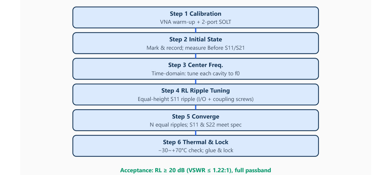
Factory tuning follows a six-step flow (Figure 4): calibration, initial measurement, center-frequency correction, RL ripple tuning, iterative convergence, and thermal aging plus locking.
5.3 RL Acceptance Criteria
| Application Grade | Min. RL | Max. VSWR | Max. Mismatch Loss |
|---|---|---|---|
| Satellite / mmWave | ≥ 20 dB | ≤ 1.22:1 | ≤ 0.04 dB |
| 5G base station Sub-6 | ≥ 18 dB | ≤ 1.29:1 | ≤ 0.07 dB |
| Telecom (general) | ≥ 15 dB | ≤ 1.43:1 | ≤ 0.14 dB |
| Amateur / commercial min. | ≥ 14 dB | ≤ 1.50:1 | ≤ 0.18 dB |
6. Case Study: S11 Before vs After Tuning
6.1 Case Background
A 6-pole coaxial cavity BPF: center 3.5 GHz, bandwidth 60 MHz (FBW ≈ 1.7%), target RL ≥ 20 dB, Chebyshev equal-ripple. After fabrication, tolerances left the initial RL out of spec; three tuning rounds met the standard.
6.2 Tuning Process Log
6.3 Before / After Comparison
| Metric | Before | After | Spec | Pass |
|---|---|---|---|---|
| Passband center | 3.512 GHz (+12 MHz) | 3.500 GHz | 3.500 ±5 MHz | Yes |
| Worst in-band RL | 11.3 dB (VSWR 1.74:1) | 21.4 dB (VSWR 1.19:1) | ≥ 20 dB | Yes |
| S11 ripple pattern | 4, asymmetric | 6, equal & symmetric | N equal | Yes |
| Insertion loss | 0.72 dB | 0.48 dB | ≤ 0.5 dB | Yes |
| Bandwidth (−3 dB) | offset | 59.2 MHz | 60 ±5 MHz | Yes |
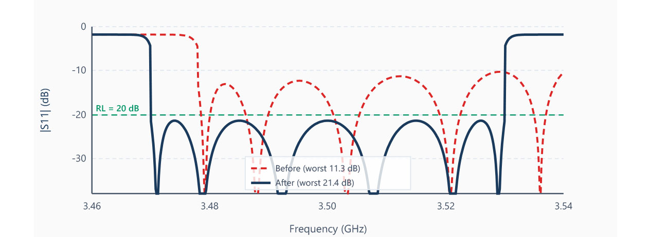
After tuning, RL improves from 11.3 dB to 21.4 dB (a 10.1 dB gain) and insertion loss falls from 0.72 dB to 0.48 dB, confirming the comprehensive benefit of precise tuning.
7. Conclusions: Best Practices for Return Loss Improvement
Tuning layer (best practices):
- Always calibrate before measuring (full SOLT 2-port).
- Time domain first, frequency domain to finish; align nulls cavity-by-cavity.
- Small steps (1/16–1/8 turn) to avoid over-shoot.
- Tune center frequency first, then RL.
- Work from the symmetry axis outward, tuning symmetric cavities together.
- Use S11 linear format to judge equal ripples.
- Both S11 and S22 must pass — never ship on one port.
- Confirm over temperature, then pot the screws.
Following this process, the TEMWELL Standard Cavity BPF stably achieves the factory standard of full-passband RL ≥ 20 dB (VSWR ≤ 1.22:1), meeting the demanding matching requirements of 5G base stations, satellite communications, and microwave systems.
★References
- A. Pons-Abenza et al., "Design and Implementation of Evanescent Mode Waveguide Filters Using Dielectrics and Additive Manufacturing Techniques," IEEE Trans. MTT, 2019 (arXiv:1909.00723).
- A. Boyer de la Giroday, "Automatic Fine Tuning of Cavity Filters," Master Thesis, Linköping University, LIU-IDA/LITH-EX-A--16/036--SE, 2016.
- W. Xia, "Diplexers and Multiplexers Design by Using Coupling Matrix Optimisation," Ph.D. Thesis, University of Birmingham, 2015.
- F. Liang, S. Meng, W. Lyu, "Design of Microwave Ceramic Waveguide Filter with High Out-of-Band Rejection," Journal on Communications, 42(4), 2021, DOI:10.11959/j.issn.1000-436x.2021029.
- T. Su, "Coupled-Resonator Circuits and the Coupling Matrix," Xidian University (technical notes).
- D. M. Pozar, Microwave Engineering, 4th ed., Wiley — Ch.2 (Return Loss, VSWR) & Ch.8 (Coupled Resonator Filters).
- R. J. Cameron, C. M. Kudsia, R. R. Mansour, Microwave Filters for Communication Systems, 2nd ed., Wiley, 2018.
- Keysight Technologies, "Filter Tuning Using Time-Domain Transforms," VNA Application Note.
- TEMWELL Corporation, Cavity Bandpass Filter Product Catalog & Technical Datasheets, smp.temwell.com, 2026.